

Arduino Pong, Part 1: The display
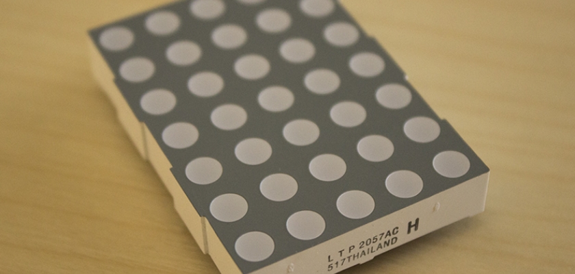
As mentioned in my last post, I've been learning up electronics with the Arduino. I found a few 5 by 7 LED matrices at a local surplus store (pictured above), so I figured another fun beginner project would be creating a clone of pong using a few of these for the screen.
After some quick research (googling the part number) I learned that the LEDs in these units are arranged in a grid pattern, with rows sharing anodes and columns sharing cathodes. Meaning, to light up all the LEDs in a single row, we provide power to only that row and ground all seven columns. The way this is designed, we can decide what LEDs we want lit in only a single row (or column) at a time. So, when an image is displayed using the entire matrix what actually happens is a single column/row is lit up at a single instant and this is applied to reach row as are scanned down through hundreds of times per second, so it looks to the human eye that the LEDs are on constantly. Another nice advantage of this is power savings - even though an LED in the grid appears to be on constantly, it's actually only on for 1/5th of real time (or 1/7ths depending on how you want to use the matrix - scanning by row or column).
I wanted a bigger screen than a single 5 by 7 matrix, so I'm stacking two right next to each other to form a 10 by 7 display. Since we now have 10 rows, we have 10 input pins. I can tie the ground (output) connection of correlating columns together so the entire screen still has only 7 ground pins. So, however we choose to run the screen's logic, we will need to "push" 17 bits to the screen - 10 to describe the input state, and 7 to describe the output state. Let's focus on setting that up first.
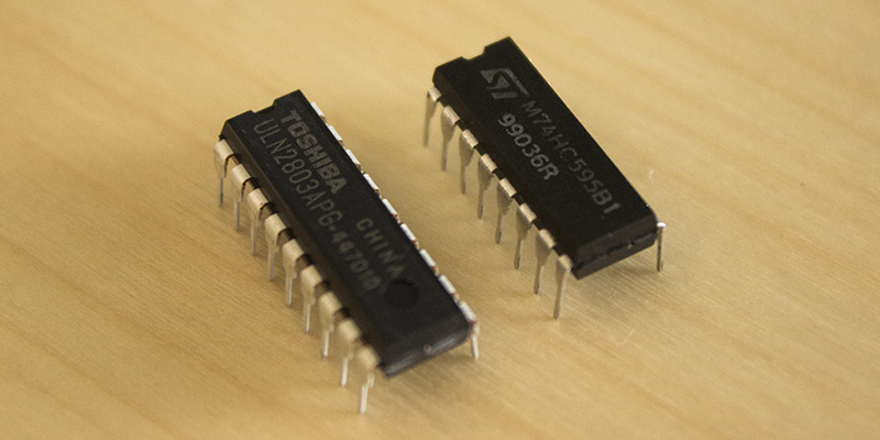
I decided to use a 74HC shift register, pictured on the right above. This chip provides 8 outputs that we can control using just three inputs (plus a power source, ground, etc of course). The shift register has an internal state, known as a register. When we "push" bits into the chip they are added at the beginning of the register, and existing bits cascade down (bit 0 moves to position 1, bit 1 moves to position 2, etc. The bit in the last position is dropped). Our data bits are signaled at pin 14, known as SI or "serial data input".
To tell the chip that there's a bit waiting on SI, we change pin 12 (RCK or "storage register clock input") from 0v to 5v. The chip recognizes this change and copies the single bit from SI to the internal register. Then, when we want the chips' 8 output pins to reflect the state of the internal register, we simply change pin 11 (SCK or "shift register clock input") to 5v. Again, the chip recognizes this change and updates the output.
There's also pins to clear the register or toggle the chips ability to output anything at all but for we don't need that functionality. They can be ignored by either tying them to ground or a 5v source, whichever the chip demands.
However, we will use another feature of the 74HC, located on pin 9 (QH or "serial data output"). When the 8ths bit is cascaded and "dropped" off the chip, it's actually sent out this pin. If the bit is 1, this pin will go HIGH for an instant, and stay LOW for a 0. This is exactly the kind of input the chip expects on pin 14, SI! This lets us chain as many shift registers as we want - QH of the leading chip to SI of the following chip, rinse and repeat. We also need to connect RCK and SCK of all the shift registers used, as the signal to read the next bit and display state all need to happen in sync.
Since I need 17 bits to control my screen, I'll need to chain 3 shift registers. On a breadboard, that looks a like this:

Quick explanation:
- The dense mixed color wires across the bottom are outputs, as well as the two green wires, and the grey one in column 57.
- The vertical orange wires provide +5v to the chips power input and other pins that need a constant 5v.
- The yellow wires ground pins called "Enable". Self explanatory.
- Pin 8 (lower right of each chip) is grounded (not pictured).
- The three blue wires in the upper right are SI, RCK, and SCK (left to right). These would go to our microcontroller.
- The horizontal orange wires is connecting QH of the leading chip to SI of the following chip (two instances of these).
- The horizontal grey wires connect the RCK pins of all 3 chips together, and the SCKs all together.
Cool! We could connect resistors LEDs to the 17 outputs (or all 24 - I don't need the last 7) to see how it works, but I'll leave that as an exercise for the reader.
We now have the ability to selectively provide power to the 10 rows of our matrix, but what about grounding the 7 columns? We need to be able to translate the 5v signal from 7 of our bits into a some logic: 5v means ground the coressponding column, and 0v means leaving the column unconnected. A basic way to do this would be a relay. A relay is like a pushbutton, but to "hold" the switch on we provide current to the relay, which it forces through a coil to create a magnetic field pulling two pieces of metal together to complete a circuit.
However, there are two problems that prevents using a relay for this case: Relays are slow: it physically moves a piece of metal to connect the circuit. We need to toggle the state hundreds of times per second; this would wear out a relay very quickly, if one could even keep up. Second problem, relays require higher current to trigger. More than we can safely provide from the 74HC registers at least. Sure, we could toggle a transistor using our register, and use that to control a strong power source, but that's unnecessary complication.
The solution: Darlington pairs. These are simply two transistors connected in a way where we can toggle grounding of one input by providing voltage to the other. Transistors require much less power than relays, and can act much faster. We have 7 outputs to control so we'd need 14 transistors in 7 pairs. Unfortunately this would take up a large amount of physical space, at least 21 rows on our breadboard. Too much.
Enter the ULN2803 (left, pictured above). This chip contains 8 Darlington pairs is one tiny package - perfect! Mine happens to be a Toshiba brand, but they come in many, many flavors. We simply connect the 7 outputs from our screen to pins 12-18, and 7 connections from our shift register bank to input pins 1-7. And, most importantly, ground pin 9. Now, to write some code!
#define DS_PIN 2
#define STCP_PIN 10
#define SHCP_PIN 11
#define NUMREG 17

boolean registers[NUMREG];

boolean screen[10][7] = {
  {1,1,1,1,1,1,1},
  {1,0,0,0,0,0,1},
  {1,0,0,0,0,0,1},
  {1,0,0,0,0,0,1},
  {1,1,1,1,1,1,1},
  {1,0,0,0,0,0,0},
  {1,0,0,0,0,0,0},
  {1,0,0,0,0,0,0},
  {1,0,0,0,0,0,0},
  {1,0,0,0,0,0,0}
};

void setup() {
  // Mark 3 pins for output
  pinMode(DS_PIN, OUTPUT);
  pinMode(STCP_PIN, OUTPUT);
  pinMode(SHCP_PIN, OUTPUT);
}

void writereg() {
  // Writes the 17 registers to the shift register bank
  digitalWrite(STCP_PIN, LOW);
  for(int i=NUMREG-1;i>=0;i--) {
    digitalWrite(SHCP_PIN, LOW);
    digitalWrite(DS_PIN, registers[i]);
    digitalWrite(SHCP_PIN, HIGH);
  }
  digitalWrite(STCP_PIN, HIGH);
}
void writescreen() {
  // Reads the screen array and manipulates regsters[] for each row
  // For each column in the row
  for(int i=0;i<=10;i++) {
    // First, blank the registers
    for(int rs=0;rs<17;rs++) registers[rs]=false;
    // Mark the column on
    registers[9-i]=true;
    for(int r=0;r<7;r++) {
      // mark any leds on
      if(screen[i][r]) registers[r+10]=true;
    }
    // Push the result to the screen
    writereg();
    // Leave this frame on for a short time
    delayMicroseconds(100);
  }
}

void loop() {
  // Write one frame to the screen, forever
  writescreen();
}
This code is pretty simple too. First, we define which pins are what. Then, create an array of 17 booleans that will be what we manipulate in the chips memory before pushing it out to the shift registers. In my setup, the first 10 bits represent row state, and the last 7 represent column state. For ease of use, we'll create a 10 by 7 multidimensional array of booleans, 1 to 1 scale with LEDs on our screen. I set it up to show a "P" (for pong!) by default, and to confirm all our rows and columns are connected and working.
In setup(), we tell the arduino which pins are which. Writereg()'s purpose is to push our in-memory array of 17 bits out to the shift registers. Writescreen() calls writereg() once per row of the screen, for one screen "refresh". Loop() calls this forever so we see the P on our screen.
Bingo!

Coming up in part two: Tracking user input!